Support for the SeeedStudio GD32 RISC-V board. More...
Detailed Description
Support for the SeeedStudio GD32 RISC-V board.
Overview
The Seedstudio GD32 RISC-V Dev Board is a development board for the GigaDevice GD32VF103VBT6 MCU with the following on-board components:
- GD32VF103VBT6 RISC-V MCU @108MHz
- 8MB on-board Flash W25Q64
- 256 byte EEPROM
- LCD Interface: 16-bit 8080 interface and SPI touch screen control interface
- USB Type C
- TF card slot
- 2 user buttons
- 3 user LEDs

Hardware:
| MCU | GD32VF103VBT6 | Supported |
|---|---|---|
| Family | RISC-V with ECLIC | |
| Vendor | GigaDevice | |
| RAM | 32 kByte | |
| Flash | 128 KByte | |
| Frequency | 108 MHz | |
| Power Modes | 3 (Sleep, Deep Sleep, Standby) | yes |
| GPIOs | 80 | yes |
| Timers | 5 x 16-bit timer | yes |
| RTC | 1 x 32-bit counter, 20-bit prescaler | yes |
| WDT | 2 x 12-bit counter, 3-bit prescaler | yes |
| ADC | 2 x 12-bit units, 16 channels @ 1 Msps | yes |
| DAC | 2 x 12-bit channel | yes |
| UART | 2 | yes |
| USART | 3 | yes |
| SPI | 3 | yes |
| I2C | 2 x Fast Mode 400 kHz | yes |
| I2S | 2 | no |
| CAN | 2 x CAN 2.0B with up to 1 Mbps | no |
| PWM | 6 Channels | yes |
| USB | 1 x USB FS OTG | yes |
| Vcc | 3.0V - 3.6V | |
| Datasheet | Datasheet | |
| Reference Manual | Reference Manual | |
| Board Manual | Board Manual | |
| Board Schematic | Board Schematic |
Pin Layout / Configuration
The general pin layout is shown below.
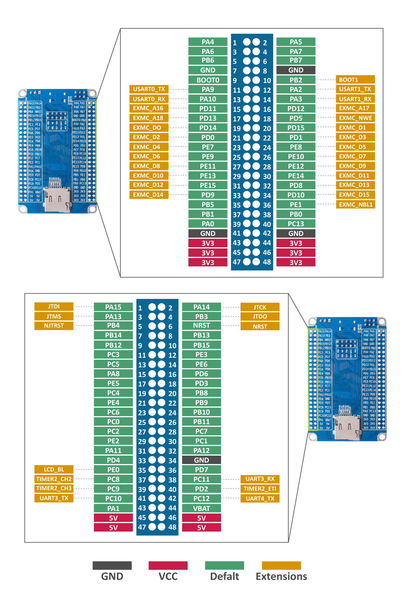
The following tables show the connection of the on-board components with the MCU pins and their configuration in RIOT sorted by RIOT peripherals and by pins.
| RIOT Peripheral | MCU Pin | MCU Peripheral | Board Function | Remark |
|---|---|---|---|---|
| ADC_LINE(0) | PA1 | ADC01_IN1 | ||
| ADC_LINE(1) | PA2 | ADC01_IN2 | ||
| ADC_LINE(2) | PA3 | ADC01_IN3 | ||
| ADC_LINE(3) | PC0 | ADC01_IN10 | ||
| ADC_LINE(4) | PC1 | ADC01_IN11 | ||
| ADC_LINE(5) | PC2 | ADC01_IN12 | ||
| ADC_LINE(6) | PC3 | ADC01_IN13 | ||
| ADC_LINE(7) | PC4 | ADC01_IN14 | ||
| ADC_LINE(8) | PC5 | ADC01_IN15 | ||
| ADC_LINE(9) | - | ADC01_IN16 | internal Temperature channel | |
| ADC_LINE(10) | - | ADC01_IN17 | internal VFEF channel | |
| BTN0 | PA0 | BOOT0 | KEY1 | |
| BTN1 | PC13 | KEY2 | ||
| I2C_DEV(0) SCL | PB6 | I2C0 SCL | ||
| I2C_DEV(0) SDA | PB7 | I2C0 SDA | ||
| I2C_DEV(1) SCL | PB10 | I2C1 SCL | ||
| I2C_DEV(1) SDA | PB11 | I2C1 SDA | ||
| LED0 | PB5 | LED red | ||
| LED1 | PB0 | LED green | ||
| LED2 | PB1 | LED blue | ||
| PWM_DEV(0) CH0 | PB0 | LED1 green | ||
| PWM_DEV(0) CH1 | PB1 | LED2 blue | ||
| PWM_DEV(1) CH0 | PB8 | N/A if CAN is used | ||
| PWM_DEV(1) CH1 | PB9 | N/A if CAN is used | ||
| SPI_DEV(0) CS | PB12 | SPI0 CS | ||
| SPI_DEV(0) SCLK | PB13 | SPI0 SCLK | ||
| SPI_DEV(0) MISO | PB14 | SPI0 MISO | ||
| SPI_DEV(0) MOSI | PB15 | SPI0 MOSI | ||
| SPI_DEV(1) CS | PA4 | SPI1 CS | ||
| SPI_DEV(1) SCLK | PA5 | SPI1 SCLK | ||
| SPI_DEV(1) MISO | PA6 | SPI1 MISO | ||
| SPI_DEV(1) MOSI | PA7 | SPI1 MOSI | ||
| UART_DEV(0) TX | PA9 | USART0 TX | UART TX | |
| UART_DEV(0) RX | PA10 | USART0 RX | UART RX |
| Pin | Board Function | RIOT Function 1 | RIOT Function 2 | RIOT Function 3 |
|---|---|---|---|---|
| PA0 | KEY1 | BTN0 | ||
| PA1 | ADC_LINE(0) | |||
| PA2 | ADC_LINE(1) | |||
| PA3 | ADC_LINE(2) | |||
| PA4 | FLASH CS | SPI_DEV(1) CS | ||
| PA5 | FLASH SCK | SPI_DEV(1) SCLK | ||
| PA6 | FLASH MISO | SPI_DEV(1) MISO | ||
| PA7 | FLASH MOSI | SPI_DEV(1) MOSI | ||
| PA8 | ||||
| PA9 | UART_DEV(0) TX | |||
| PA10 | UART_DEV(0) RX | |||
| PA11 | USB D- | |||
| PA12 | USB D+ | |||
| PA13 | JTAG TMS | |||
| PA14 | JTAG TCK | |||
| PA15 | JTAG TDI | |||
| PB0 | LED green | PWM_DEV(0) CH0 | LED1 | |
| PB1 | LED blue | PWM_DEV(0) CH1 | LED2 | |
| PB3 | JTAG TDO | |||
| PB4 | JTAG NRST | |||
| PB5 | LED red | LED3 | ||
| PB6 | I2C_DEV(0) SCL | |||
| PB7 | I2C_DEV(0) SDA | |||
| PB8 | PWM_DEV(1) CH0 | |||
| PB9 | PWM_DEV(1) CH1 | |||
| PB10 | I2C_DEV(1) SCL | |||
| PB11 | I2C_DEV(1) SDA | |||
| PB12 | SD CS | SPI_DEV(0) CS | ||
| PB13 | SD SCK | SPI_DEV(0) SCLK | ||
| PB14 | SD MISO | SPI_DEV(0) MISO | ||
| PB15 | SD MOSI | SPI_DEV(0) MOSI | ||
| PC0 | ADC_LINE(3) | |||
| PC1 | ADC_LINE(4) | |||
| PC2 | ADC_LINE(5) | |||
| PC3 | ADC_LINE(6) | |||
| PC4 | ADC_LINE(7) | |||
| PC5 | ADC_LINE(8) | |||
| PC13 | KEY2 | BTN1 | ||
| - | Temperature | ADC_LINE(9) | ||
| - | VREF | ADC_LINE(10) |
All other pins are either not broken out or have no special usage.
Flashing the Device
The board is flashed via a JTAG interface with OpenOCD (at least release version 0.12.0). By default, an FTDI adapter according to the configuration defined in interface/openocd-usb.cfg is assumed.
To use an FTDI adapter with a different configuration, the configuration can be defined using the variable OPENOCD_FTDI_ADAPTER, for example:
If another adapter is used, it can be specified using variable OPENOCD_DEBUG_ADAPTER, for example for a Segger J-Link adapter:
Accessing STDIO
By default, the stdio is provided by the USBUS CDC ACM module stdio_cdc_acm. This interface is mapped to /dev/ttyACM<n> on a Linux host, where <n> is the index of the CDC ACM interface, which is 0 by default.
To use the first UART interface for stdio instead, the stdio_uart module has to be enabled:
The stdio is then directly accessible through the first UART interface. If an external USB-to-UART interface is used, this interface is mapped to /dev/ttyUSB<n> on a Linux host, where <n> is the index of the UART interface, which is 0 by default.
Use the term target to connect to the board using /dev/ttyUSB0:
If the UART interface index of the USB-to-UART interface is not 0, use the following command to connect:
Files | |
| file | board.h |
| Board specific definitions for the SeeedStudio GD32 RISC-V board. | |
| file | gpio_params.h |
| Configuration of SAUL mapped GPIO pins. | |
| file | periph_conf.h |
| Board specific definitions for the SeeedStudio GD32 RISC-V board. | |
